

Result description
Customizable, sustainable, and industry-ready photovoltaic technology: A reproducible and scalable methodology has been developed for the industrial fabrication of thin-film photovoltaic devices based on CZTSe, using only non-toxic and earth-abundant materials. This technology enables customization of both physical design and power output, making it ideal for tailored applications in products and power supply systems for IoT devices. A sustainable and versatile solution that meets the emerging needs of the tech sector for local in-situ energy generation and the digitalization of society.
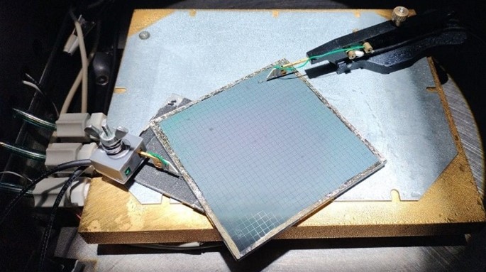
A reproducible and scalable methodology has been developed for the industrial production of thin-film photovoltaic (PV) devices based on CZTSe absorbers, using only non-toxic and earth-abundant materials. The technology achieves a power generation density of 8 mW/cm² under standard AM1.5 illumination. This sustainable PV solution allows customization of both the physical design and power output, making it especially suitable for decentralized energy applications and IoT devices. In fact, it can directly power a Zigbee communication system with just 1 cm² of active area. The manufacturing process is based on optimized sequential sputtering and annealing steps, compatible with medium-scale industrial production. The technology has been validated over 10×10 cm² areas, demonstrating high homogeneity with a power output dispersion of less than 5 %, as measured by 3×3 mm² calibrated test cells distributed across the full surface
Addressing target audiences and expressing needs
- Collaboration
- Business Angels
- Venture Capital
· Business partners – SMEs and industrial players in the PV, IoT and smart device sectors
· System integrators – for embedding CZTSe PV in autonomous or low-power electronic systems
· Manufacturing partners – for pilot-scale production of thin-film CZTSe modules
· Technology adopters – companies developing energy-autonomous IoT products
· Funding bodies / Investors – to support scale-up and market entry
- Public or private funding institutions
- Research and Technology Organisations
- Private Investors
R&D, Technology and Innovation aspects
The CZTSe-based thin-film photovoltaic technology has been developed and optimized through sequential sputtering and annealing. It has been validated at lab scale on 10×10 cm² substrates, showing <5% power dispersion and achieving 8 mW/cm² output under AM1.5. Functional demonstration in powering Zigbee-based IoT devices has been achieved. Next steps involve system development and integration.
The process is based on industrially scalable techniques such as sputtering, compatible with roll-to-roll and batch production systems for thin-film PV manufacturing.
The methodology is reproducible and transferable to other production environments and compatible with a variety of low-cost, flexible, or rigid substrates.
The technology uses non-toxic, earth-abundant materials and avoids critical raw materials. It supports energy autonomy, reduces environmental impact, and contributes to multiple UN SDGs (7, 9, 12, 13).
- Global
- North America
- Europe
- Asia
Result submitted to Horizon Results Platform by FUNDACIO INSTITUT DE RECERCA DE L’ENERGIA DE CATALUNYA