Optical sensors are pervasive. For example, digital cameras using CMOS detectors have been indispensable vacation companions for many years. In industry they serve as a simple and economical solution for automated image processing (such as in quality control applications, remote presence and position recognition and counting in conveyor systems, or object recognition in warehousing logistics). They can also be employed in medical engineering for diagnostic image processing. There are many future applications in the field of autonomous vehicles that are already foreseeable today.
Motivation
The detectable spectral range of CMOS sensors often is limited to the visible wavelength range. However, the applications mentioned above partly need detection outside this range – for example in the nearinfrared (NIR) range.
This functionality usually is realized by hybrid solutions such as a combination of indium gallium arsenide (InGaAs) detectors on CMOS readout circuits. Nevertheless, the manufacturing of these kinds of hybrid solutions is considerably more costly, which limits the use in some applications.
Solution
Organic photodiodes offer an interesting alternative because they can be monolithically integrated at wafer level on top of highperformance CMOS readout circuits.
Fraunhofer IPMS has extensive experience in integrating organic layers on CMOS wafers. Until now the focus was set on the integration of emitting layers for OLED microdisplays. This know-how in processing can also be used for the integration of organic photodiodes (OPD).
Demonstrator
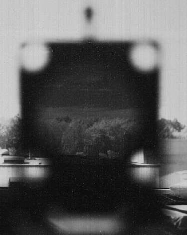
A first ASIC has been developed for demonstration purposes, which offers the possibility to read out an organic layer with SVGA-resolution (800 × 600 pixels). This image sensor was fabricated completely at wafer level and therefore already under production-like conditions. With its extended region of sensitivity, the imager can be employed over the entire bandwidth of conventional applications in industry, the automotive sector, and medicine. Possible application examples include driver assistance systems, food quality control, optical fingerprint sensors or biomedical tests.
The implemented demonstrator forms a platform for customer-specific sensor developments, which are made possible by adapting and optimising the organic layer system. At the same time, it makes it easier to get started with this type of development, as an existing development environment consisting of an ASIC readout chip, control electronics and software can be used.
Our offer
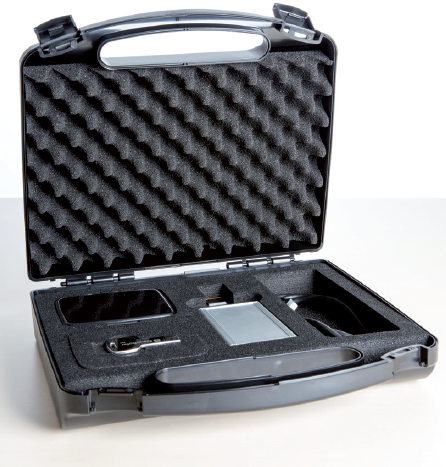
- Evaluation kit of an initial OPD sensor including readout electronics by USB interface and easy to use configuration of the image sensor via configuration software
- Evaluation of organic sensor layers
- Customer specific adjustment of the organic sensor layer system according to the application-specific needs and wavelengths
- CMOS backplane design for adjustment of the sensor performance like e.g. resolution, pixel- and sensor size, framerate or to comply with specific organic layers
- Application studies of new image sensors based on organic photodiodes
Fraunhofer IPMS is ready and available for customer-specific developments, prototyping and manufacturing of small series. Together with an established manufacturing partner we can also offer higher volume quantities commercially.


