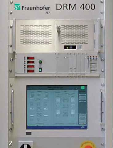
We use sputter technologies and high-rate PECVD to develop processes for depositing optical, electrical, acoustic, and magnetic layers and layer systems precisely and homogeneously on large substrates at high coating rates.
In particular, applications in the areas of optics, electronics, sensor technology, solar energy, and medical technology require uniform coatings of high quality with few defect sites on large areas or on large numbers of substrates. Our long-term stable sputter processes are ideal for manufacturing these precision layer systems. We have extensive experience with reactive gas feed control, process control, and in-situ quality monitoring and are thus able to carry out reactive processes highly reproduceable.
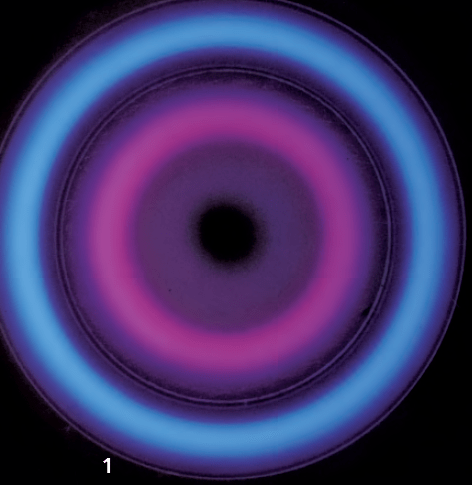
The equipment CLUSTER 300 can coat stationary substrates having a diameter up to 12“ (300 mm). There are double ring magnetrons in the coating chambers. The superposition of their inner and outer discharge rings allows homogeneous layer thicknesses and layer property distributions to be achieved. Furthermore, gradient layer systems can also be deposited, which for certain applications have better properties than multilayer systems.
The cluster equipment can also be used to apply metals, alloys, multilayer systems,
compounds, and hybrid systems of metals and organic compounds to glass, silicon wafers, metal surfaces, and films with high process reliability.
Our offer
- Development and optimization of coating technologies and layer systems for your applications
- Development of key components (magnetron sputter sources, plasma-etching units) customized for specific coating tasks
- Coating of samples and pilot production
- Transfer of integrated packages (comprising key components, fully automatic control systems, and technology) to production plants
- Support with cost determination and technical realization


