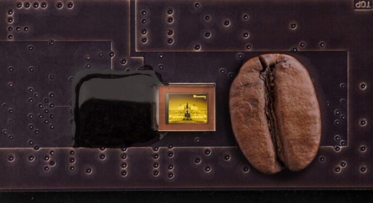
OLED microdisplays have so far been developed predominantly on 200mm wafers. These conventional CMOS technologies and the associated backplane design have limited the number and size of pixels until now. At the Fraunhofer Institute for Organic Electronics, Electron Beam and Plasma Technology FEP, OLED microdisplays have been realized for the first time in a 28-nanometer backplane technology on 300mm wafers within the “Backplane” project funded by the Saxon State Ministry of Economics, Labor and Transport (SMWA). Components with a display diagonal of 0.18 inches and pixel sizes of only 2.5 micrometers have been manufactured. This corresponds to a pixel density of 10,000 dpi – an as-yet unattained level in the global OLED microdisplay market. These unique OLED microdisplays will be presented for the first time at SID Display Week, May 23–25, 2023, at the German Joint Booth, No. 1110, in Los Angeles, USA.
The working group for microdisplays has moved to Fraunhofer IPMS.

