Applications
The variability of substrates and the ability to deliver a complete development and production cycle allows the technology to be used in such areas as:
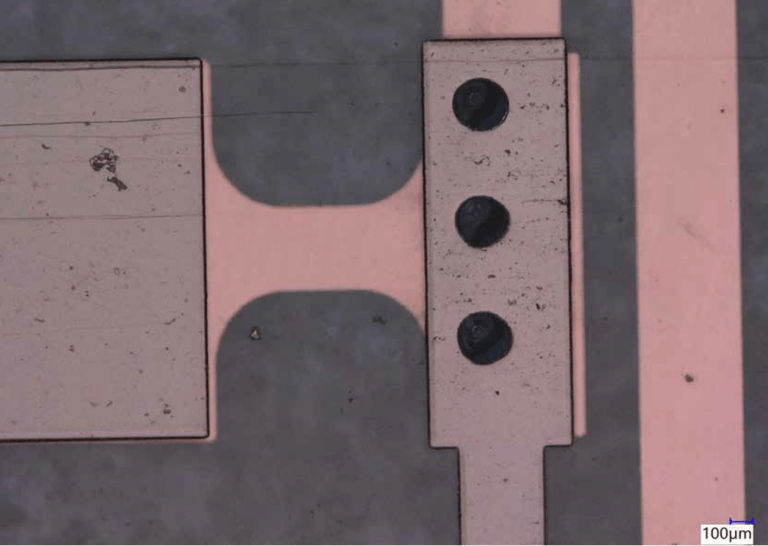
- Flexible circuit boards and multilayer structures with interconnects and resolution down to 10 μm
- High-density fine-line technology for chip assembly
- Low-loss and high accuracy antennae for high frequency applications
Fraunhofer EMFT services
Fraunhofer EMFT provides an extensive portfolio of process „know-how“ for R2R production of flexible electronics. This includes for example:
- In-house sputtering on PET and PI foils up to a web width of 215 mm
- Web ultrasound cleaning and drying
- Dry resist hot press lamination
- Digital double-sided photolithography exposure
- Wet development and etching
- Plasma surface cleaning and surface modification
- Laser ablation, via process and engraving
- Laser cutting
- R2R bare die pick-and-placement
- Electrical and mechanical foil-to-foil assembly and packaging
These modules can be combined at will, depending on the requirements of the application in question. Parameters such as structural precision can be individually tailored to the customer requirements.


