Deposition of highly insulating layers by magnetron sputtering
Some materials, like aluminum oxide (Al2O3), silicon dioxide (SiO2) and silicon nitride (Si3N4) show excellent electrical insulation properties with high specific resistance and high dielectric strengths of some MV/cm (megavolts per centimeter).
At Fraunhofer FEP, we have developed reactive magnetron sputter processes to deposit such insulating layers with high deposition rates of 2 – 4 nm/s. This allows economical deposition of layers from a few hundred nanometers up to several (ten) micron thickness, with break down voltages of more than 2000 V. This was proven on very different substrates, ranging from Silicon wafers to hardened steel or rough Cu substrates. The reactive magnetron sputter process uses metal targets, like silicon or aluminum in a mixed argon-reactive gas atmosphere.
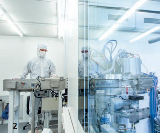
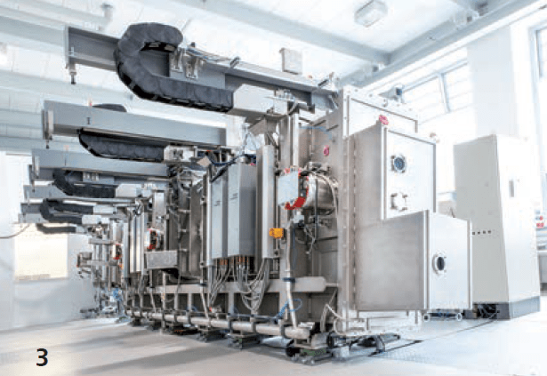
Different deposition plants are available at Fraunhofer FEP equipped with two types of magnetron sources for layer deposition: a double ring magnetron source (DRM 400) for stationary coating of substrates up to Ø 200 mm and a rectangular magnetron (RM 800) for dynamic coating of larger substrates up to 650 mm × 750 mm. Substrates to be coated can be flat or 3D parts.
Our offer
Complete project chain from feasibility studies and technology development to transfer of hardware and technology to customer.


