Are you looking for a flexible, focused, objective and yield-oriented partner to bloom up your idea till the device proof of concept?
The INL MNF Facility is your key partner from the early stage of the design conception till the last phase. It unfolds from the process integration and development to the most expert process engineers on the latest core technologies. MNF Facility is prepared for small pre-productions series, facilitating technology transfer to industry and their standardization also in multi-project wafers (MPW).
What do we offer in our facilities?
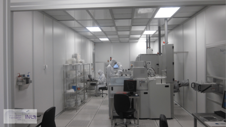
- Open-access and service provider cleanroom of 700 m2 offering cutting-edge capabilities and interdisciplinary solutions for 200 mm wafer down to samples of less than 10mm in size,
- Support throughout all the development chain in cleanroom processes: device modelling and design, process integration and device fabrication, packaging and testing,
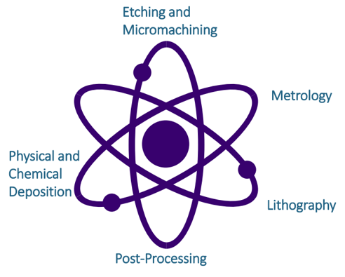
- Core fabrication areas:
-
- (Thin) Film Deposition and growth of materials (sputtering, CVD, ALD and electroplating);
- Etching, ashing and micromachining (RIE and Deep RIE, isotropic etch, Wet etch and, O2 plasma strip);
- Optical and E-Beam Lithography (from µm below to 10nm resolution, fast pattern replication & inversion of patterns);
- Advanced packaging, Annealing and back-end: processes (CMP, dicing, SCPD);
- In-line process metrology, inspection and characterization and testing (SEM, OPM, OM, Thin film resistivity, Profilometer, Interferometer).
