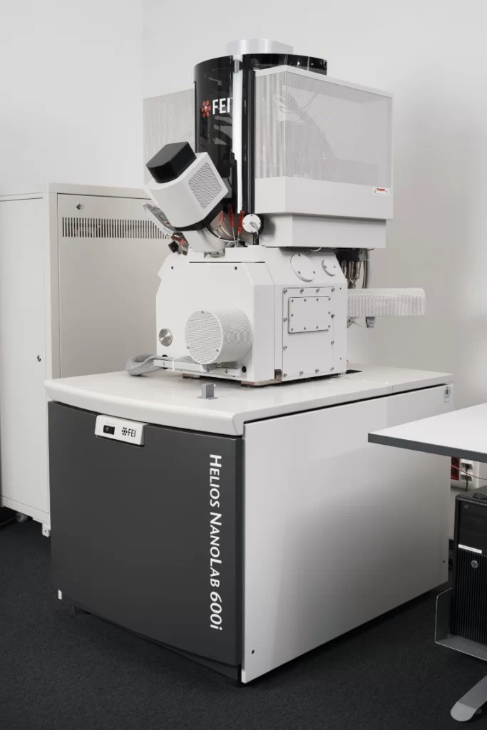
The FEI dual beam SEM/Ga-FIB microscope combines the advantages of an ultra high-resolution electron microscope and an ion microscope. It can therefore be used for high-resolution imaging and as a material processing tool. The energy of the focused beam of gallium ions allows for the preparation material to be selectively removed and modified at the nanoscale. This is related to the possibility of making cross-sections, 3D reconstruction and TEM samples preparation, as well as prototyping processes in nano- and microscale. Available detectors: ETD, TLD, CBS and EDS.
PARAMETERS
Landing voltage range:
- electron beam: 350 V – 30 kV (50 V – 30 kV with Beam Deceleration mode),
- ion beam: 500 V – 30 kV.
Resolution:
- electron beam: 1 nm,*
- ion beam: 2,5 nm.*
Maximum sample size:
- diameter: 150 mm diameter with full rotation (assembly possible of larger preparations*),
- height: 100 mm,
- weight: 500 g (including the sample holder).
DETECTORS
- ETD (secondary electrons)
- TLD (secondary electrons)
- ICE (secondary ions)
- CBS (backscattered electrons)

