Chips for Organic Field Effect Transistors (OFET)
Substrates for Material Characterization
Organic semiconductors are key components in organic electronics and photovoltaics.
They are used to create flexible electronic devices and solar cells that convert sunlight
into electricity. Their unique properties offer advantages such as flexibility and
environmentally friendly, low-cost manufacturing.
Typical for this class of materials are low temperature processes and large area deposition and structuring with various coating and printing processes. The active semiconductor materials determine the performance of the entire system considerably. That is why an easy-to-use and reliable electronic characterization of these semiconductors is an essential prerequisite for material and process developers.
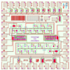
Fraunhofer IPMS offers standardized and customer-specific transistor structures in
bottom-gate architecture. These substrates enable the characterization of conducting and semiconducting materials like organic semiconductors for thin-film gas sensors. They are essential for material development and testing as well as for quality control. Optimum measurement results can be achieved by adapting the chips in terms of chip size, design and dielectric layer thickness.
The following properties are mostly of interest:
- Conductivity
- Charge carrier mobility
- Contact resistance
- On/Off current ratio
To simplify the measurement procedures of OFET substrates, Fraunhofer IPMS has also developed a hand prober. This OFET miniprober allows fast and easy measurements by reliable pad contacting.
Chips for Organic Field Effect Transistors (OFET)
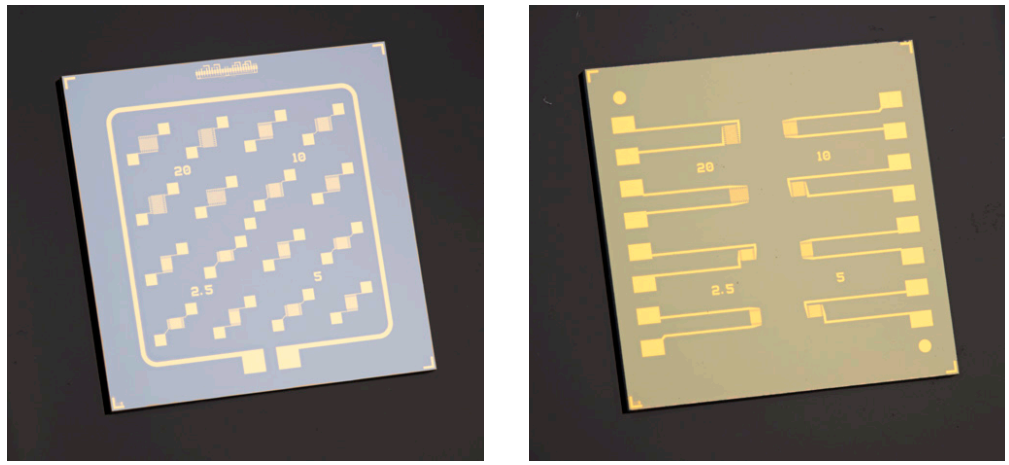
If an organic semiconductor layer is deposited on such a substrate, the Si-bulk acts as gate electrode and controls the channel current between the gold electrodes on top. A suitably doped Si-SiO2 interface in CMOS quality guarantees a reproducible gate contact. Gold electrodes with a patented undercoating suppress the formation of injector barriers between the gold electrodes and the organics in the transistor channel. This guarantees reliable ohmic source / drain contacts in the OFET even for p-type semiconductors. Due to both reliability and reproducible preparation, these substrates are applied for standardized material screening by all key developers of organic semiconductors all over the world.
Advantages
- Various designs and channel sizes on one chip
- Large channel lengths possible
- Different orientations of the transistors
- High reproducibility and precision
- Adjustable gate oxide thickness
- Low leakage current
- Top gate contact for easy contacting
OFET Miniprober
Easy to use and quick measurements without expensive prober stations. With a given substrate size, pad grid and pad arrangement in large batches, Fraunhofer IPMS has developed a miniprober (top right). It has two electric connections on the front (source and drain) and one connection on the back (gate) and does not require probe station, samplers or manipulator pins. A reliable interconnection is established on contact pads, which are only 0.5 × 0.5 mm² in size. Customized versions of the miniprober varying the connection arrangement, the position and number of the pads are possible. This makes the miniprober suitable for other applications in addition to OFETs. Signals are transmitted to the measurement instrument by BNC or triax cables.
Advantages
- No probing system required
- Easy DUT handling
- Stable and secure connection
- Other chip sizes or pad arrangements possible