Direct-write micropatterning OLEDs using electron beam technology
Fraunhofer IPMS is investigating the effects and possible applications of electron beam technologies in the field of organic electronics. During this research, a novel approach was developed by which any fabricated OLED device can be patterned individually and at high resolution. The patented technology uses an electron beam process, which takes place after finalizing the OLED including the encapsulation. Therefore it is possible to build the OLED highly productive and completely unpatterned, before the emission is individually modified by an adjusted electron beam process.
The penetrating electrons of the electron beam lead to a local reduction in charge carrier injection. This permanently reduces the local emission level compared to its initial level, which simultaneously results in reduced power consumption.
The process is highly adaptable – regardless of whether the OLED is applied to a rigid medium or a flexible film, what color the OLED is, or whether the substrate is optically opaque, translucent, or transparent. The size of the substrate is universal as well and can be matched to the corresponding application.
The energy of the accelerated electrons determines their penetration depth into the OLED layer stack. A suitable accelerating voltage is selected to specifically deposit the triggering electron energy at a level below the encapsulation layer. This enables the modification of the luminous characteristics of the organic layers without destroying or damaging the encapsulation itself. Depending on the application, even individual organic layers can be directly targeted. Lateral control of the electron beam permits any shape to be structured.
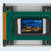
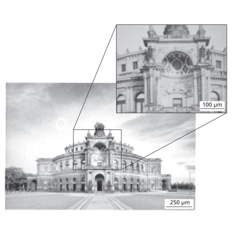
The electron dose determines the degree of change in emissivity. The greater the dose, the darker the affected location appears. This allows a continuous range of intensities to be created on monochrome OLEDs.
To estimate the penetration depth of the electrons into the OLED layer stack and the energy absorption, specific layer properties and scattering processes at the interfaces must be taken into account. At Fraunhofer IPMS, Monte Carlo simulations are used to estimate these complex electron-solidstate interactions, which allow statements to be made about the energy absorption in the individual layers of the OLEDs produced at the institute.
It turns out that most of the energy is absorbed in the encapsulation layers and only a fraction reaches the sensitive organic layers. By increasing the acceleration voltage, the influenced proportion of the organic layers can be increased and at the same time the electron dose for a desired change in emissivity can be reduced.