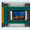
Thin film deposition, structuring and analysis on wafer level (200 mm)
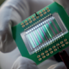
Fraunhofer IPMS disposes of a wide array of processes available under cleanroom condition. The equipment is geared to the development and manufacturing of OLED microdisplays. The main focus lies on the deposition and structuring as well as the patterning of organic and inorganic layers from the nm up to the µm range. Several tools and processes are available for this purpose. In addition, we offer analytical methods for thin film characterization.
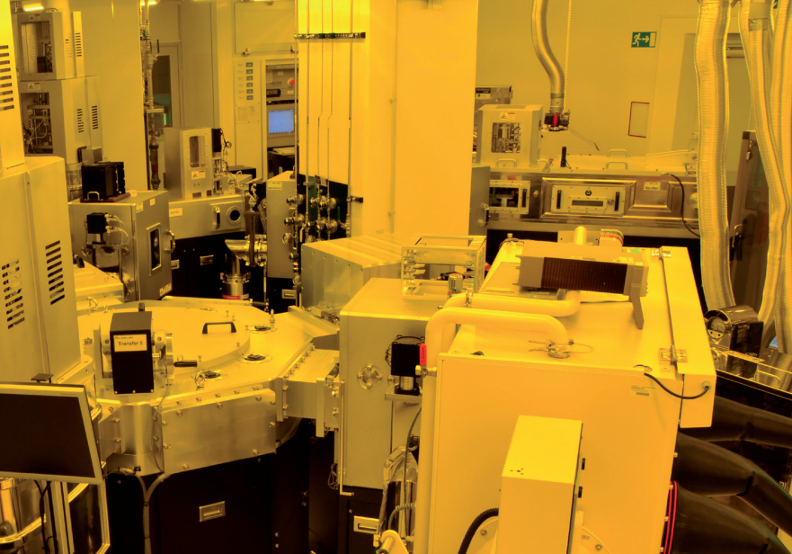
Processes, technologies and equipment under cleanroom condition ISO 5
At Fraunhofer IPMS we have the opportunity to combine different processes and tools. Layer and layer stacks can be thin film encapsulated to protect them from moisture and oxygen, if needed.
We can also combine evaporated and spincoated materials with various anode / cathode materials to be finally encapsulated and structured on pilot line quality.
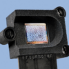
Another highlight is the alignment accuracy of ±10 µm for shadow masks during layer deposition and argon etching.
Besides layer deposition and structuring, the bonding of wafers and substrates is an important process. Color filter wafer can be aligned with an accuracy of ±1 µm and bonded under vacuum. In addition, there are processes for temporary bonding available.
- Deposition of single layer and layer stacks
- Particle measurement
- Structuring of layers
- Bonding
- Photo lithography
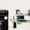
- Electro-optical tests
- Electro-optical characterization (Wentworth wafer prober)