
Wafer-level micromagnets
Technology
Magnetfab’s patented technology is based on more than 16 years of research at Institut Néel – CNRS Grenoble, which is one of the world’s top research institutions in the field of magnetism.
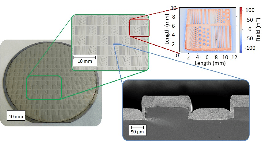
Unlike the traditional fabrication approach for magnets that relies on powder metallurgy, we produce micromagnets by means of sputtering, a technique which consists in depositing thin film layers that is widely used for manufacturing optical coatings and semiconductor devices.
Utilizing state-of-the-art microfabrication equipment within a controlled clean-room environment, we can achieve microscale precision in patterning our sputtered magnetic films. This capability enables us to produce thousands of micromagnets with unrivaled uniformity and submicron-level shape control, all seamlessly integrated onto a single wafer.
What sets our magnetic films apart is that they consist of Neodymium Iron Boron (NdFeB), an alloy based on rare-earth elements known for possessing the highest energy density among all known magnetic materials. Notably, NdFeB is the very same permanent magnet material employed in over 90% of contemporary electric vehicle traction motors. The robust and strong static magnetic field of NdFeB magnets even finds application in guiding and shaping beams of particles moving at nearly the speed of light within particle accelerators.
Applications
Just as LEDs have revolutionized lighting and transistors have empowered computing, micromagnets hold the promise of disrupting microsystems, most prominently represented by microelectromechanical systems (MEMS). The importance of using permanent magnets in microsystems lies in their ability to enable miniaturization, energy efficiency, and precise control of magnetic fields at the microscale. This opens up a wide range of applications in fields like in medtech, portable consumer devices, microfluidics, robotics, sensing, and in quantum technology, where the integration of magnetic functionality is essential for achieving desired performance and functionality in micro-sized devices.
Magnetfab’s wafer level micromagnets enable advanced products such as:
- Microspeakers
- Cell phone cameras with optical image stabilization
- Tactile sensors
- MEMS micromirros for augmented reality
- Automotive position sensors
- Haptic feedback deices
- Magnetic field sensors
- Microfluidic devices such as micropumps or droplet manipulation
- and more…