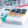
Precision Coating
Precision coating
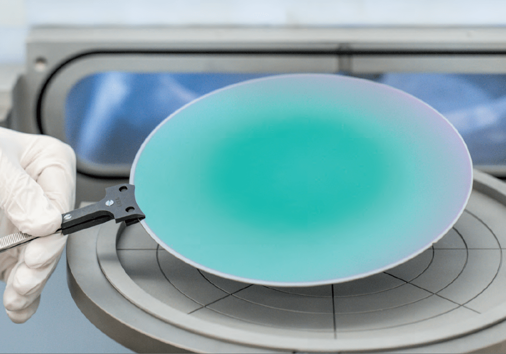
Many applications in the field of optics, electronics, sensors, energy and medical technology require highly precise coatings. Fraunhofer FEP develops deposition hardware and technologies for fabrication of those optically, electrically, acoustically and magnetically effective layers and layer systems. The pulse magnetron sputtering and magnetron PECVD processes are optimized concerning precision and long term stability as well as high deposition rate and uniformity even at large substrates. The combination of these processes with precise substrate movement and optical in-situ monitoring ensure reproducible coating properties and precise layer thicknesses.
Reactive pulse magnetron sputtering (PMS) and magnetron PECVD
With reactive PMS, it is possible to deposit compound layers with a high layer quality at high deposition rate. In this process, electrically conductive targets are sputtered while reactive gas (e.g. O2, N2, F2, NH3) or a mixture of them is introduced. The layer is formed out of the atomized target material and its reaction with the reactive gas on the substrate surface. The deposition rate is usually one magnitude higher than the one achieved by RF sputtering from the compound target. In contrast, during the magnetron PECVD process, a precursor is introduced (e.g. SiH4, HMDSO, TEOS). The plasma causes chemical reactions and the deposition of inorganic, organic or hybrid layers on the substrate. No or only a very low quantity of the target material is atomized and incorporated into the layer. The deposition rate is up to one magnitude higher than the one achieved with reactive PMS.
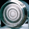
Dynamic / stationary coating
During dynamic sputtering a substrate passes by the sputtering station. This procedure is usually preferred if large substrates or a large number of small substrates arranged on a carrier are to be coated in in-line deposition plants. The substrate remains in front of the sputtering station during stationary sputtering processes. This process is usually preferred for deposition of layers on single substrates (currently for substrates with a diameter up to 300 mm and for substrates with a diameter up to 450 mm in future) or on several small substrates arranged on a carrier in cluster deposition plants.
Our offer
- development and optimization of coating technologies, reactive sputtering processes and coating systems for your applications
- coating of samples and pilot production
- development of key components such as magnetron sputter sources, plasma-etching sources
- Our offerprocess-control units adapted to the requirements of the coating tasks
- transfer of integrated packages, consisting of key components, fully automatic process and control systems as well as technology, into production plants
- assistance with cost estimation and technical implementation into deposition plants