Report Abuse

Mikroskop-SEM_Xe-PFIB-FEI-Helios-G4-PFIB-CXe-683×1024-1

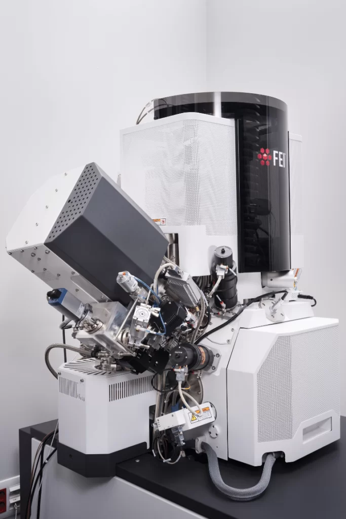
SEM/XE-PFIB FEI HELIOS G4 PFIB CXE MICROSCOPE

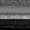
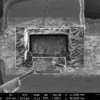
Helios G4 PFIB CXe is a dual beam microscope with an electron column and an ion column that generates a xenon ions beam. Xenon plasma focused ion beam (Xe-PFIB) technology allows for new tests, unattainable by other methods. In combination with an ultra-high-resolution electron microscope and a fast EDS detector from Bruker, it is the only such analytical system commercially available in Poland. It is distinguished, among others, by up to 50 times faster work than in the case of gallium technology (Ga-FIB), no ion implantation and compatibility with most materials – including aluminum samples and gallium-containing samples. Available detectors: ETD, TLD, ICE, ICD and EDS.

PARAMETERS

Landing voltage range​:

  • electron beam: 50 V – 30 kV,
  • ion beam: 2 kV – 30 kV.

Resolution:

  • electron beam: 1 nm,*
  • ion beam: <25 nm.*

Maximum sample size:

  • diameter: 150 mm diameter with full rotation (assembly possible of larger preparations*),
  • height: 100 mm,
  • weight: 500 g (including the sample holder).
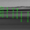
DETECTORS

  • ETD (secondary electrons)
  • TLD (secondary electrons)
  • CBS backscattered electrons)
  • ICE (secondary ions)
  • EDS (characteristic X-rays*)

Deliverables

Specifications and Deliverables
– The ultra-high-resolution imaging of surface preparation.
–  Create maps of elemental EDS, analysis of point and linear elemental composition.
– Creation and analysis cross-sections in nano- and microscale.
– Selective application of materials in FEBID and FIBID technology.*
– Imaging contrast material preparation.
– The ability to characterize a wide range of formulations of conductive and non-conductive without modifying them,*
– Three-dimensional reconstruction of the specimen on the basis of SEM images (approximately 1 000 µm3 volume).
– Preparation of high-quality TEM samples with a thickness of less than 100 nm – compatibility with the materials based on aluminum and gallium.
– Rapid prototyping of spatial structures in nano- and microscale.
– Etching material without leaving artifacts (e.g. implanting gallium).

Contact Listings Owner Form

Premium Feature Preview: see who has visited your listings (only for logged-in users)

Last 20 users who visited this post

user photo viewed this listing at 2024-03-15 10:15:58
user photo Bartek Rusecki viewed this listing at 2024-04-18 14:15:55